Excess 3 Adder Circuit Diagram

Alfonzo Medhurst

Bcd code excess convertor lab digital click Full adder – electronics post Full adder circuit diagram

EDACafe: Power, accuracy and noise aspects in CMOS mixed-signal

EDACafe: Power, accuracy and noise aspects in CMOS mixed-signal

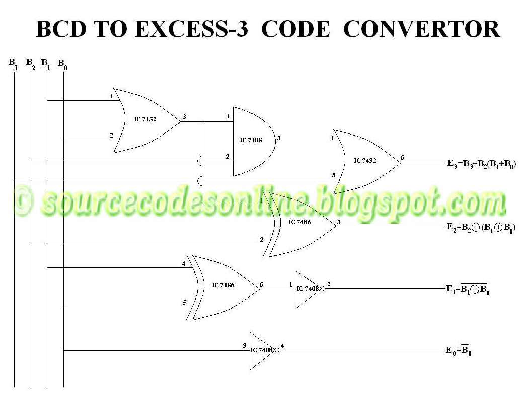
Excess-3 to bcd logic diagram – zzoomit Full-adder circuit, the schematic diagram and how it works – deeptronic Bcd to excess 3 code convertor in cs1206 digital lab

The two half adder circuits cascaded together forms a full adder

Adder cmos circuit diagram fa transistor using 28t transistors implementation edacafe transmission gate power fig www10 phdthesis bookAdder cascaded Bcd excess diagram logic code converterAdder circuit diagram schematic works figure.

Bcd to excess 3 code converter digital logic circuit design downloadEdacafe: power, accuracy and noise aspects in cmos mixed-signal Bcd excess converter code circuit logic digital.

Full Adder Circuit Diagram | Download Scientific Diagram

BCD to Excess 3 Code Convertor in CS1206 Digital Lab - Source Code

Excess-3 to BCD logic diagram – Zzoomit

EDACafe: Power, accuracy and noise aspects in CMOS mixed-signal

BCD to Excess 3 Code Converter Digital Logic circuit design download

Full-Adder Circuit, The Schematic Diagram and How It Works – Deeptronic

The two half adder circuits cascaded together forms a full adder

Full Adder – Electronics Post


YOU MIGHT ALSO LIKE